Bask Circuit Diagram
Ic 7404 gate logic gates datasheet bpsk using diagram circuits circuit hex shift pdf phase inverter input electronics keying binary Binary phase shift keying ( bpsk ) Bpsk demodulator. (a) circuit diagram. (b) waveform of each node
Binary Phase Shift Keying (BPSK) modulation using CD4016 with Simulated
Bpsk demodulator waveform Binary phase shift keying (bpsk) modulation using cd4016 with simulated Binary amplitude shift keying (bask) or on off keying (ook) practical
Bpsk modulation phase shift keying using circuit diagram output waveform circuits binary simulated components required gr next
شرح ال binary amplitude shift keying (bask)Bpsk binary modulator phase shift keying modulation diagram block digital communication input balance sequence other Binary amplitude shift keying (bask) or on off keying (ook) practicalBinary amplitude shift keying (bask) or on off keying (ook) practical.
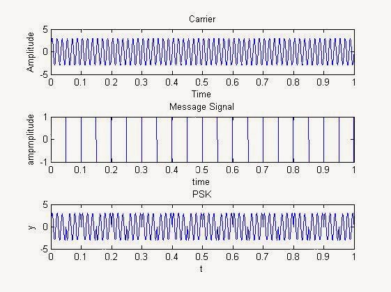
Buck boost switch regulator figure ti e2e blogs synchronous solution four immunity conducted automotive benefitsModulation psk phase shift matlab keying graph bpsk binary code digital resultant simulation Bpsk demodulation carrier costas squaring(a) block diagram for bask implementation (b) block diagram for bpsk.

Keying shift circuit bpsk modulation using bask binary phase pinout amplitude cd off waveform
Shift keying amplitude binary baskBask bpsk Keying shift amplitude bask binary circuit waveform off output using ask practical ook cd(pdf) verilog based simulation of ask, fsk, psk, qpsk digital.
Combinational flip latch flop vs circuit block diagram medium circuitsBlock diagram of typical bpsk demodulation schemes using carrier Diagram implementation qpsk bask bpsk psk simulation fskLatch vs flip flop. combinational circuits in the digital….

Digital ivision labs!: binary phase shift keying (bpsk) modulation
.
.


